The microcode ROM was always going to be a wiring problem. Every instruction looks up a 64-bit control word: what the ALU should do, whether to write a register, read memory, jump the PC, enable multiply, and so on. In simulation that's one chip and one splitter. On a breadboard it's twenty-something wires crawling across the whole CPU—and the signals don't even go where you'd expect. Shift mode comes out of the ALU decode block but plugs into mul-div. Flag-write enable lives with the memory controls but feeds the ALU. PC jump fields are split across two bytes in the ROM. Fine on paper, miserable to route.
Before
One microcode.dig on main. One big EEPROM, one 64-bit splitter, every control line tunnels out from the same place.
What worked: One ROM file, one address bus (ir_opcode from the IR), dead simple in Digital. Change an opcode row, one place to edit.
What hurt: Fanout hell. To test mul-div you need the entire decode tree running. Long ribbons from the center of the board to ALU, memory, PC, shift unit. Touch the bit layout and you're redoing a 64-wide splitter and re-homing every net at once.
Current
Split decode into small boards—same idea as alu-control, the first one I built. Each board sits next to the hardware it actually drives. They all listen to the same 10-bit opcode from the IR; that's the shared backplane. Each board has its own small 8-bit EEPROM and a local splitter.
- ALU control — ALU opcode, operand prep, carry select. Lives on the ALU board.
- Shift / mul-div control — shift mode, multiply enable, priority-encoder mux. Lives on the mul-div board. One ROM row merges fields that used to sit in different bytes of the big word, so I'm not duplicating chips just for two wires from the ALU board.
- IR / register / writeback control — which immediate encoding to use, where writeback data comes from, register write enable.
- Memory I/O control — bank select, mem read/write, byte lane select. Flag-write enable comes out here too—one wire over to the ALU, can't be helped.
- Memory bus control — what goes on the address bus (PC? ALU result? stack pointer?) and how store data is picked.
- PC / stack control — branches, jumps, PC source, link register, cycle count, branch conditions, stack pointer ops. Two small ROMs here because those fields don't pack into one byte without cutting something in half.
HALT stays on main—opcode 0x3FF plus execute phase. One comparator, not worth its own board.
The Advantages
- Short ribbons. Decode happens where the logic is.
- Bring-up in pieces. I can validate the ALU board with just ALU control before the rest exists.
- The master opcode catalog stays the source of truth; a script cuts per-board ROM images from it. Packed rows where the old byte boundaries were awkward, straight slices where they weren't.
The Cons
- Eight EEPROMs instead of one. Opcode fans out to all of them.
- ROM data in the boards is still pasted wrong in places—truncated 64-bit junk instead of proper 8-bit images. Needs a proper extract step.
Next Steps: Clean up duplicate ROMs in ALU control, generate real per-board hex from the catalog, run the exhaustive microcode test.
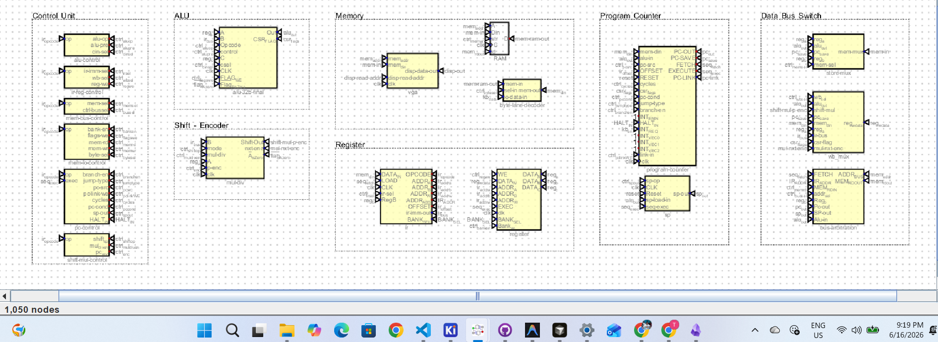
Final design of main
All six control boards are in the Control Unit block on main—decode sits with the datapath it drives instead of one central microcode blob.
Status
main wired with alu-control, ir-reg-control, mem-io-control, mem-bus-control, pc-control, and shift-mul-control. ROM data in the boards still needs proper per-board hex from the catalog.