See also: Elimination of Mode Multiplexers · ALU Architecture Refinement · First Lights and Flux
This project soon moved into tomato.tmarhguy.com.
And the extreme optimization shifted it into a new project, rightfully so. 3488 MOSFETs for an ALU was all about the story, and the CMOS story.
It intentionally neglected the NMOS-only + pull-up resistor designs, or other exotic "non-CMOS" designs.
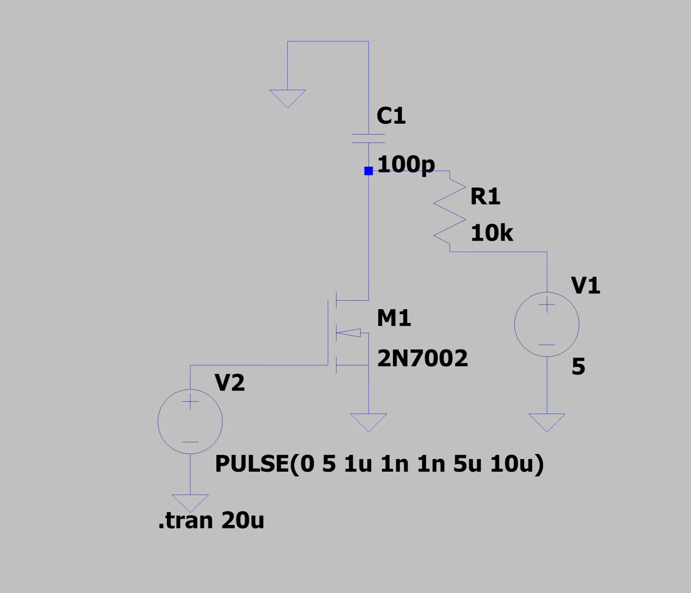
NMOS-only inverter with resistive pull-up — the topology this build deliberately skipped.
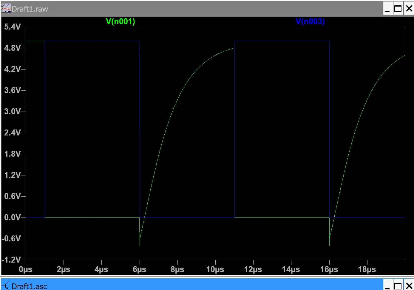
Gate pulse vs drain: slow RC recovery through the 10k when the FET turns off (100pF load).
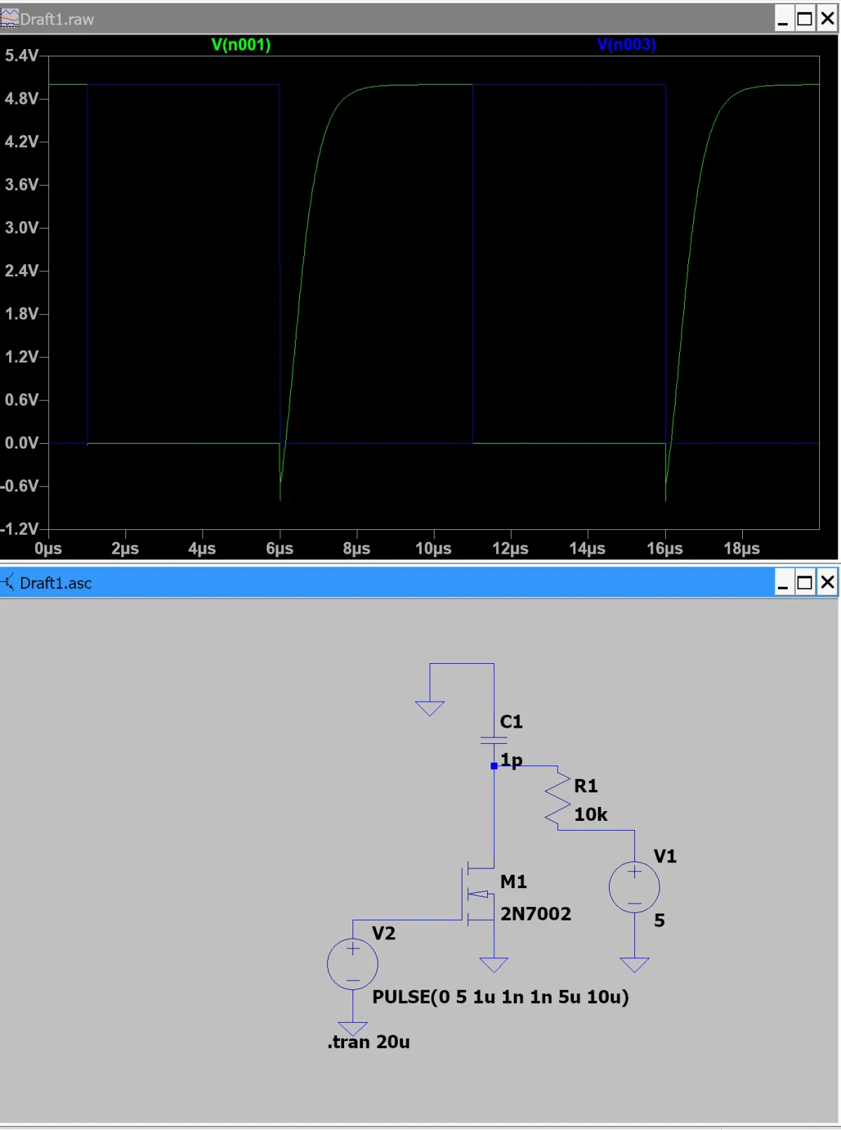
Same circuit at 1pF — pull-up recovers faster, but the story is still resistor-limited, not complementary CMOS.
I soon ran into fabrication challenges, mainly due to extreme cost explosion on the PMOS side. These were all initially accounted for, but careful reconsideration weighs the cons higher than the pros.
I have considered the following redesigns.
Reconfigure from naive opcode → decode → compute → multiplex out into dual "lut2" → full adder with a post-logic shift right.
I have out of intentionality avoided the final multiplexer at all costs as I find it redundant and unnecessary in a discrete build.
The rules at nanoscopic scales are different from macroscopic. For instance, a transistor is expensive at the macro scale, but so cheap that a wire rather is expensive at the nanoscopic scale.
The primary focus is a discrete build, and I let that ground any drifts.
For a tapeout like an ASIC flow in the future, I will consider other metrics, explore Amdahl, and other metric laws and maybe tone down clock speed favoring throughput over latency.